Introduction
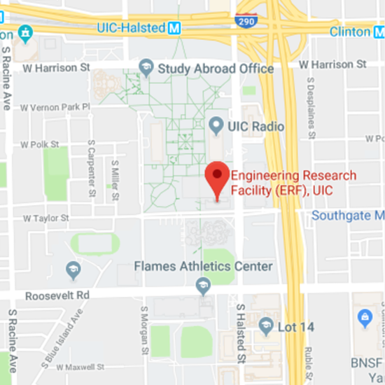
The MNFTL is housed in Room 1064 of the Engineering Research Facility (ERF), located at 842 W. Taylor St. in Chicago. The laboratory occupies 1300 ft2 of modern research space with three full-service chemical hoods and several optical tables for bench-top experiments. Available equipment includes a high-speed digital imaging system (Vision Research Phantom Miro M310), a custom-made goniometer for measurement of contact and roll-off angles, several digital cameras, three microbalances, high-intensity lighting, optical microscopes, a gas-purged glove box, an inkjet printing system for printed electronics, a modulated Differential Scanning Calorimeter, a spray robot, a temperature/humidity chamber (ESPEC SH-641), function generators, power supplies, amplifiers and other electronic devices. Several droplet generators are available for creating droplets in the size range from 50µm to larger than 1 mm. The laboratory staff is very experienced with procedures in the micro- and nano-science area, and especially in measurements pertaining to liquid repellency. MNFTL staff has access to other UIC experimental facilities supporting micro- and nanotechnology, and materials characterization research.
1
The following service facilities are within a few steps from the laboratory:
1
The UIC Research Resources Center (RRC) maintains and supports state-of-the-art equipment needed to meet the needs of UIC researchers and their external collaborators. The RRC has been providing core support for research at UIC for over 50 years. At present, its research support services consist of 20 cores, centers and laboratories, including the Electron Microscopy Service (EMS) Facility. EMS provides a comprehensive electron microscope and surface analysis facility dedicated to bringing state-of-the-art methods in modern imaging, and spectroscopy, to life and materials scientists with all levels of expertise. It is a central facility offering instrumentation, training and service using scanning (SEM & Microprobe), transmission (TEM) and scanning transmission (STEM) electron microscopy, surface analysis (XPS), oxide film growth (MBE) and vibrational spectroscopy (Raman). For technical specifications of all available instruments, click here. EMS is staffed with experts in each technique who can teach researchers to operate the instruments, in order to conduct their own measurements. Once trained, expert users have 24-hour access to the instrumentation. The EMS staff can also provide guidance, consultation, and collaboration in the application of various techniques to a user’s specimens. Equipment for material science specimen preparation includes coating, slicing, disc cutting, polishing, ultramicrotomy, electrochemical and chemical thinning and ion beam milling. EMS is a regional center of excellence for atomic-resolution STEM, having upgraded its Scanning Transmission Electron Microscopy (STEM) facility by installing a Nion aberration corrector on the VG HB601UX dedicated STEM and adding a state of the art aberration corrected JEOL ARM-200CF.
1
The UIC Nanotechnology Core Facility (NCF) is a versatile MEMS/Nano facility, which is accessible to University, non-profit and industrial researchers. The NCF enables research by providing access, training, service and process guidance on fabrication and characterization equipment. As a research and development laboratory, the NCF is dedicated to application of integrated circuit and fiber optic technology to improve manufacturing methods for MEMS/Nano devices, BioMEMS, Microfluidic, Electromechanical, Mechanical, Chemical, Optical, Photonic and multi-functional devices, some of which have previously been built by more traditional techniques. The NCF has versatile equipment for: Photolithography (Mask Making capabilities, Mid/Deep-UV, top & bottom alignment), Fabrication (DRIE for Silicon & Silica, RIE, PECVD Oxidation/ Diffusion, LPCVD, RTP, Bulk and Surface Micromachining, Sputtering and E-beam metal evaporation, Polymer deposition and processing), Metrology (AFM, Optical & Contact Profilometry, Optical Inspection, High speed camera, Thin Film Stress Measurement), and Back-end processing (Dicing, Lead attachment and die bonding).
